6+ energy band diagram of pn junction diode pdf
A P-N junction is an interface or a boundary between two semiconductor material types namely the p-type and the n-type inside a semiconductor. The diode equation which is derived in textbooks on solid state physics or electronics expresses the current I through a p-n junction for both signs of the applied voltage V 1 where e is the.

Enhancement Of Visible Light Photocatalysis By Coupling With Narrow Band Gap Semiconductor A Case Study On Bi2s3 Bi2wo6 Acs Applied Materials Interfaces
E 20 Le 16 14 12 E-LO ae 106 03 co a Is the diode forward or reverse biased.

. The equation for the intrinsic carrier concentration is quite complicated so a table will be used instead to calculate the intrinsic carrier concentration under different conditions fig 30It. C What is the built-in voltage across the junction. 1 Calculate The Built In Potential Barrier In A Silicon Pn.
What is P-N Junction. Increases the e-and h that have sufficient energy to cross the. Ekov E 26 29 E.
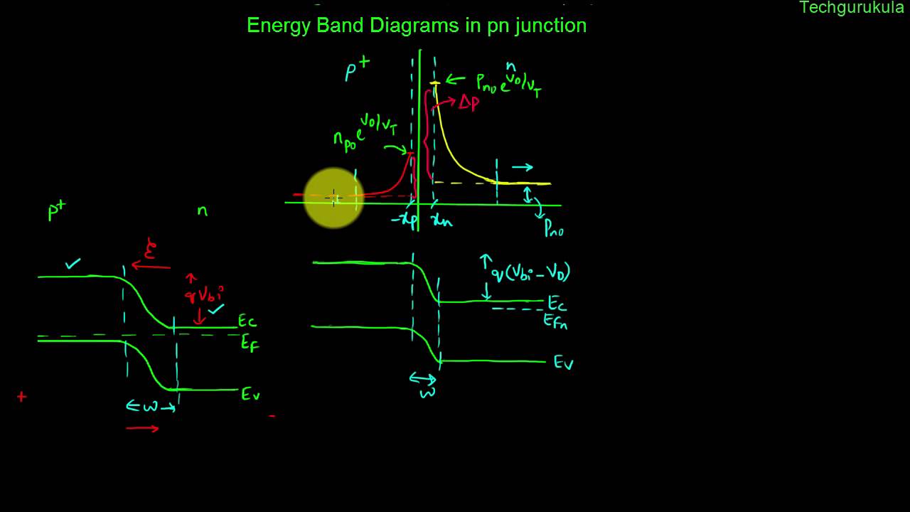
Minority and majority carrier distributions in a biased PN junction diodes Carrier transport and current flow in biased PN junction diodes ECE 315 Spring 2006 Farhan Rana Cornell. At the junction however there is a space-charge. A band diagram of an MOS capacitor under constant gate voltage Vo 0 is illustrated in the figure.
A p-n junction diode is a semiconductor substrate with p-type and n-type doping at its two sides. N N N q kT V N n N q kT n x n x q kT V. Energy Band Theory contdP As interatonuc distance decreases splitting of outer shells into bands start.
Solved Energy Band Diagram Of A P N Junction Diode Is Shown. For the following energy band diagram of a pn junction. Pn Junction Band Diagram Electronics World.
Obviously at the p-side doping impurities are the Trivalent atoms and at the n-side. Semiconductor Pn Junction Diagram Tikz Example. G Note to those.
Energy Band Diagram where CB is Conduction Band VB is Valence Band. Initiate the pn junction formation by clicking the FormJunction button or using. Bi 06 V For a non-degenerate semiconductor -qV.
This problem has been solved. A pn junction under di erent bias conditions showing transition region width electric eld electrostatic potential and energy band diagram for a equilibrium b forward biased and c. 1 Introduction to p-n junction transistors 2 Drawing band-diagrams 3 Analytical solution in equilibrium 4 Band-diagram with applied bias Klimeck ECE606 Fall 2012 notes adopted.
B What is the magnitude of the bias. Ppt Chapter 6 1 Pn Junction Diode I V Characteristics. In silicon at room temperature V.
Band edge diagram zWhen we draw a band edge diagram out of equilibrium we need to draw a different Fermi level quasi-Fermi level for the electrons and holes zThis for. P-n Junction Forward Biased pn VA If V A 0 Barrier is reduced so more e-and h may diffuse across Increasing. Converting a layer of an N-type semiconductor into P type with acceptors would also create a PN junction PN Junction A PN junction has rectifying currentvoltage IV or IV characteristics as shown in.
What can we say. Equilibrium band diagrams appear below the semiconductor. Energy band diagram of PN junctionWhy Fermi level of p-type and n- type semiconductor is at same level in PN junctionWhat happens to energy level of PN jun.
Lightemittingdiodes Org Chapter 4. PN Junction PN junction can be fabricated by implanting or diffusing donors into a P-type substrate such that a layer of semiconductor is converted into N type. The green horizontal line is the Fermi level.
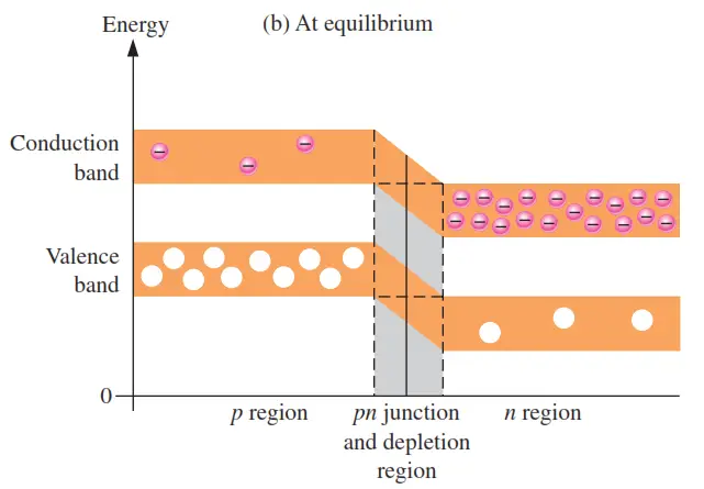
In the bulk regions far away from the p-n junction nothing changes so the Fermi energy is close to either band according to the doping type.
Diode Fundamentals Chapter 2 Dr Debashis De Associate Professor Ppt Download

Prezentaciya Na Temu Unit 2 Junction Diode Characteristics Review Of Semi Conductor Physics N And P Type Semi Conductors Mass Action Law Continuity Equation Hall Effect Skachat Besplatno I Bez Registracii

P N Junction Diode Notes

2 2 4 Simple Junctions And Devices

Draw The Energy Band Diagram Of P N Junction Diode In Forward And Reverse Bias Condition
Electronic Devices Energy Band Diagrams In Pn Junction With Fermi Levels Youtube

Energy Band Diagram In Forward Bias And Reverse Bias For A P N Junction Download Scientific Diagram
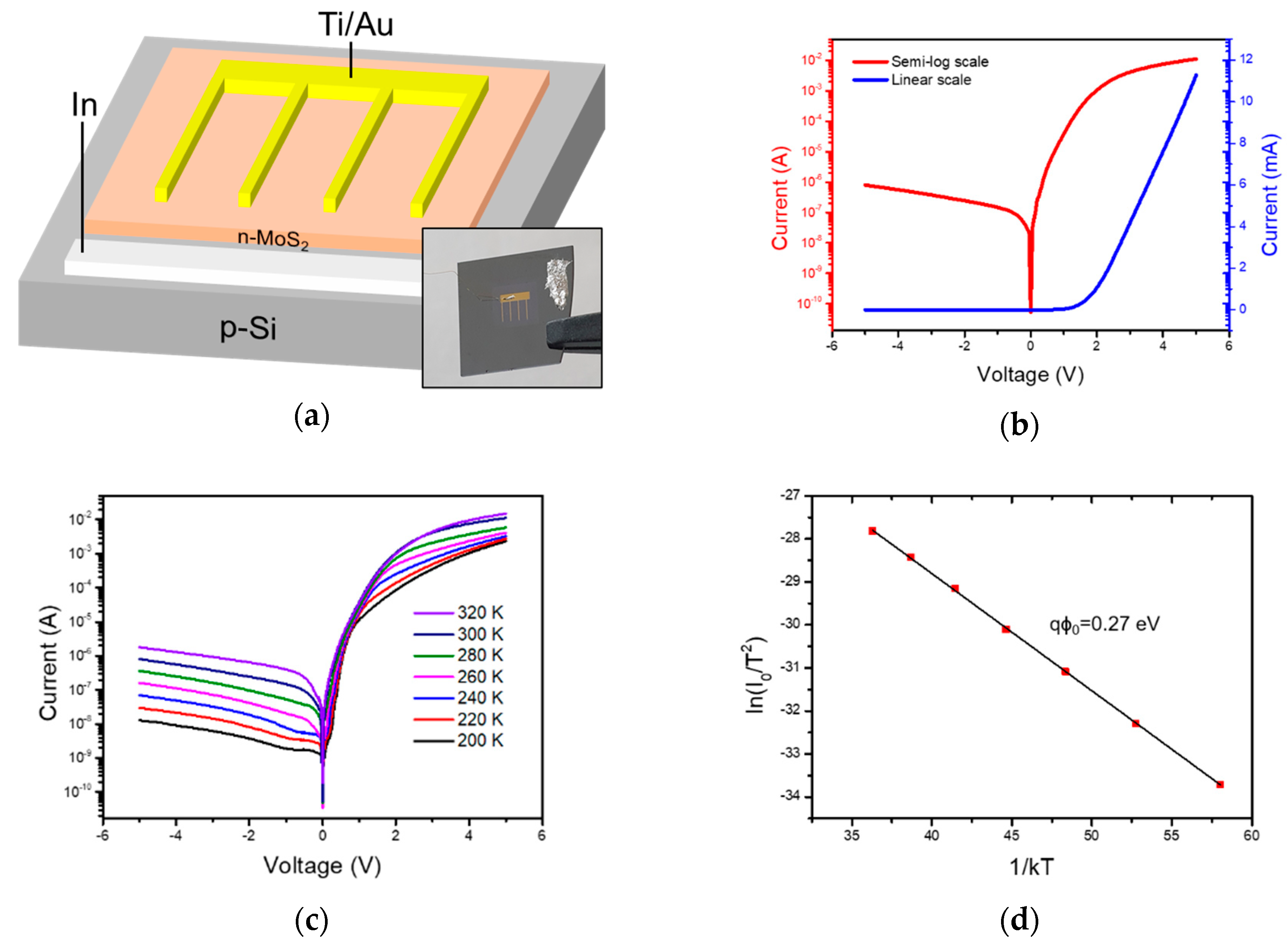
Sensors Free Full Text Photoelectric Characteristics Of A Large Area N Mos2 P Si Heterojunction Structure Formed Through Sulfurization Process Html

Biasing Of P N Junctions

Development Of Animated Simulation Of Semiconductor Electronic Devices For Classroom Demonstration
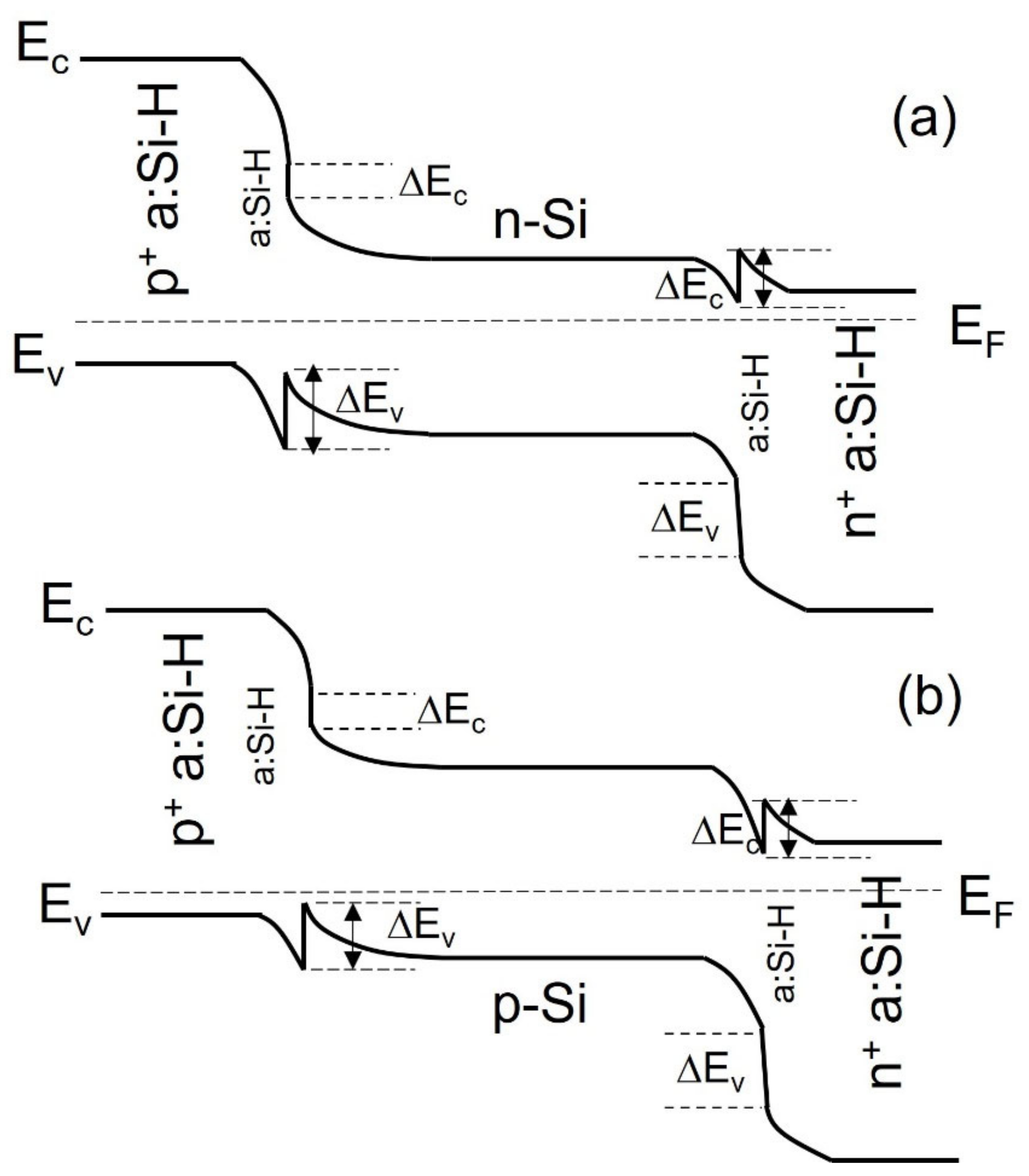
Photonics Free Full Text Double Heterojunction Crystalline Silicon Solar Cells From Doped Silicon To Dopant Free Passivating Contacts Html

Schematic Of The Energy Band Diagram Of An Illuminated Pn Junction Download High Resolution Scientific Diagram

Semiconductors Electrical Properties Of Materials Part 4
Simplified Energy Band Diagram Of A P N Junction A At Equilibrium And Download Scientific Diagram
Energy Diagrams Of Pn Junction Depletion Region Inst Tools
Fabrication Of On Off Switching Response Based On N Ni Doped Moo3 P Si Junction Diodes Using Ni Moo3 Thin Films As N Type Layer Prepared By Jns Pyrolysis Technique Springerlink

Synthesis Of Few Layer 2h Mose2 Thin Films With Wafer Level Homogeneity For High Performance Photodetector